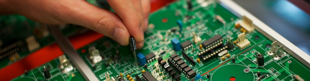
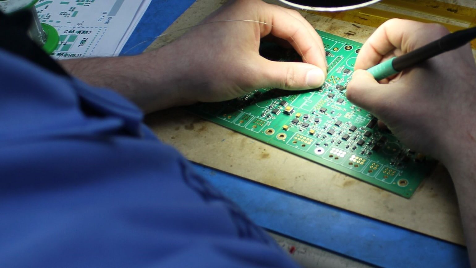
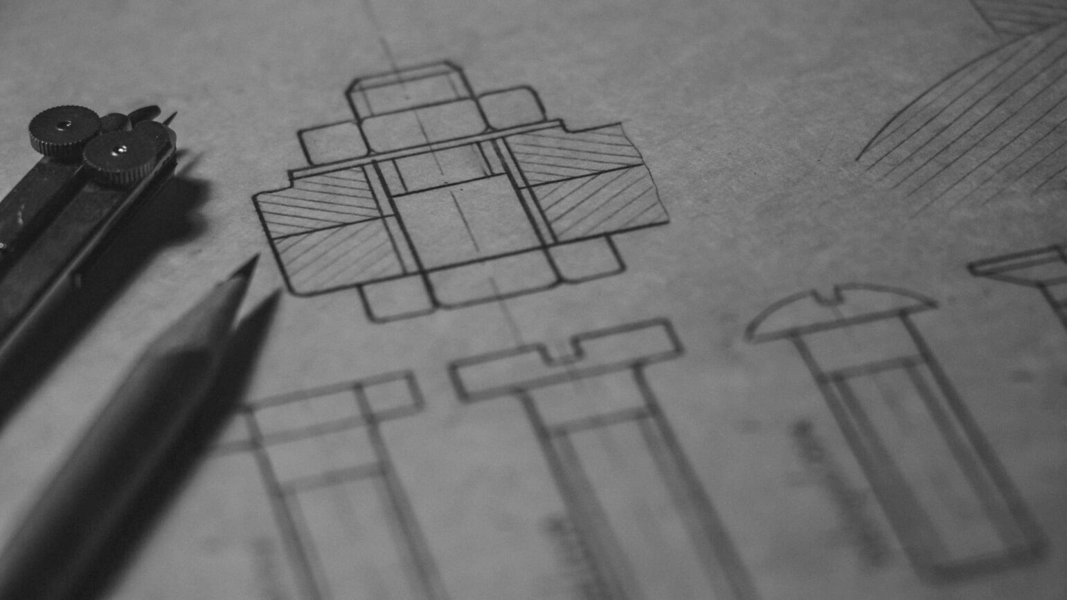
At GB Electronics, we provide a full suite of electronics design services to businesses in West Sussex and beyond, offering innovative solutions from concept through to production.
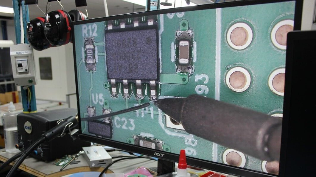
Whether you need help with schematic design, embedded systems, or full turnkey projects, our experienced electronics designers ensure your product is developed with precision and efficiency.
We work across a wide range of industries, including industrial, consumer, IoT and medical sectors, delivering customised designs that meet your exact requirements.
Contact us today to discuss your project and see how we can help bring your ideas to life.
Our electronics design service includes:
- Schematic and PCB layout using Altium® CAE software
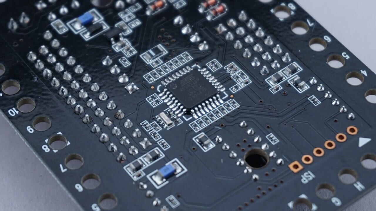
- Design for ARM microcontrollers and similar RISC devices
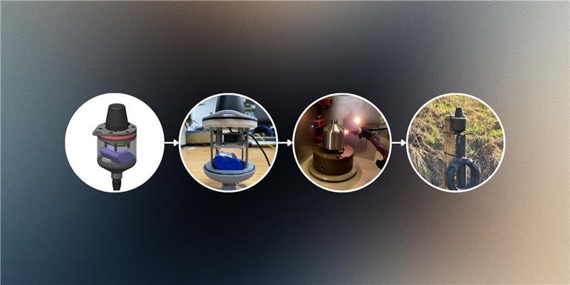
- Embedded systems and data loggers
- Full turnkey solutions and flexible work packages
- Design for Manufacturing (DfM) and production rollout
- Risk management and compliance
- Electro-mechanical integration
- Power management, including battery and solar design
- Feasibility studies and prototypes
- Product review, enhancement, and redesign
- Production programming and test tools design
- Bespoke integration for Raspberry Pi, including custom HATs